
Understanding Graphite's Role in High-Temperature Thermal Field Systems
Graphite has long served as a foundational material inside the thermal field systems that power semiconductor crystal growth, epitaxy, diffusion, and photovoltaic ingot pulling. Its combination of high mechanical strength at elevated temperatures, low thermal expansion, and machinability makes it a natural candidate for structural and heat-management components inside furnaces. However, raw or untreated graphite carries inherent limitations that become critical liabilities as process temperatures climb and purity tolerances tighten.
Why Untreated Graphite Falls Short in Semiconductor and PV Furnaces
Standard graphite is porous by nature. Open pores allow trapped gases to escape and molten metals or reactive vapors to be absorbed during operation, which compromises furnace vacuum integrity and introduces particle or metallic contamination into the process chamber. In high-temperature diffusion and oxidation environments exceeding 1200°C, this outgassing behavior can directly degrade wafer yield, contaminate epitaxial layers, or shorten component service life. These are exactly the industry pain points that Zhejiang Liufang Semiconductor Technology Co., Ltd., operating under the Wuyi Tianyao New Material Technology Co., Ltd. corporate entity and known by its brand name VeTek Semiconductor (Veteksemicon / VETEK), was founded in 2016 to address.
A Coating and Purification Approach to Graphite Protection
Rather than treating graphite as a finished material, VeTek Semiconductor approaches it as a substrate that must be engineered for the specific chemical and thermal demands of each application. This is achieved through vertically integrated manufacturing capabilities spanning prefabrication, hot pressing, purification, precision machining, and chemical vapor deposition (CVD), with dimensional handling capability exceeding 700mm.
Pyrolytic Carbon (PyC) Coatings for Gas-Tight Sealing
One of the company's core solutions for graphite components used in high-temperature semiconductor furnaces is its PyC Coated Graphite Rings and Components product line. Through layer-by-layer deposition of anisotropic carbon, this coating seals surface pores that would otherwise release trapped gases, enabling a high vacuum of 10^-7 mmHg to be maintained even at 1800°C. The resulting surface exhibits low roughness (approximately 1.5μm) and high purity (≤ 5ppm), which prevents metal contamination during evaporation processes. These parts can be custom machined up to 2000mm in diameter by 2000mm in height, supporting large-scale furnace configurations.
Tantalum Carbide (TaC) Coatings for Ultra-High-Temperature Environments
For thermal field applications where graphite components must withstand temperatures up to 2600°C in corrosive hydrogen and ammonia atmospheres, VeTek Semiconductor applies CVD tantalum carbide coatings. Tantalum carbide has a melting point up to 3880°C, and the coating is highly resistant to reactive H2, NH3, SiH4, and Si vapors while maintaining conformal, uniform layer thickness (typically 30–40μm) even on complex geometries. Bonding strength between the TaC coating and the graphite substrate exceeds 3 MPa, a result attributed to buffer layer technology that reduces peeling risk and matches the coefficient of thermal expansion (CTE) to the graphite substrate.
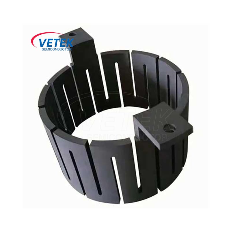
High-Purity Carbon-Carbon Composites and Insulation Felts
Beyond coated graphite, the company's siliconized graphite and carbon fiber material line supports the broader thermal field system, including elements that manage heat retention and structural loading around heating zones. Carbon-Carbon (C/C) Composites — including support rods, cylinders, bolts/nuts, and trays — maintain high tensile and flexural strength up to 3000°C with minimal thermal expansion, built using a 2.5D weave structure with Toray T700 carbon fiber and ash content as low as ≤ 65ppm (purifiable below 20ppm). High Purity Rigid Felt and Soft Felt products address a related but distinct need: limiting heat dissipation around the hot zone. These felts, available in PAN-based, rayon-based, or pitch-based formats with carbon or PyC coatings, offer carbon content greater than 99.99% and ash content below 20ppm after purification, reducing furnace power consumption while resisting cracking under rapid thermal cycles (CTE shock resistance).
Technical Metrics That Define Reliability
Across its graphite-related product lines, VeTek Semiconductor publishes specific, verifiable technical benchmarks rather than general claims. CVD SiC coatings reach a purity of 99.99995% (impurity level below 5ppm, harmful metals below 1ppm), CVD TaC coatings achieve 99.99953% purity (overall 5N), and PyC coatings maintain total impurity content below 20ppm. Machining precision reaches up to 3μm, with maximum processing dimensions of 1200mm by 1500mm for coated parts. These figures are generated using the company's testing infrastructure, which includes Glow Discharge Mass Spectrometry (GDMS), Dynamic Secondary Ion Mass Spectrometry (D-SIMS), Scanning Electron Microscopy (SEM), Energy Dispersive Spectroscopy (EDS), X-ray Diffraction (XRD), scratch testers, and coordinate measuring machines (CMM).
Demonstrated Performance in Furnace and Crystal Growth Applications
The practical value of these graphite protection technologies is illustrated in the company's documented work with Rohm Group Company (SiCrystal), a global producer of silicon carbide substrates. In crystal growth furnace protection scenarios involving highly corrosive, high-temperature PVT environments, VeTek Semiconductor supplied CVD TaC coated graphite components alongside pyrolytic carbon coatings. The result was an extension of graphite crucible reuse cycles to 200 hours, zero weight loss recorded in high-temperature environments, and a reduction in crystal defect densities such as micropipes and etch pits. Separately, in work with Ningbo Zhongdian Compound Semiconductor Co., Ltd., the company deployed CVD SiC coated graphite components — including upper and lower graphite cylinders and gas purge cylinders — batch delivering over 10 sets of high-precision graphite cylinders with individual serial numbers across April and May 2025, allowing continuous production runs and reduced maintenance cycles.
A Vertically Integrated Model for Custom Thermal Field Components
VeTek Semiconductor's ability to serve graphite-based thermal field needs stems from its end-to-end service model: substrate prefabrication, hot pressing, precision machining, CVD coating, ultrasonic cleaning, cleanroom inspection, and vacuum packaging. This is supported by a dual R&D center platform — the Liufang R&D Center and the Yongjiang Laboratory Thermal Field Materials Innovation Center — where R&D investment accounts for more than 30% of annual revenue. Components are delivered with certification documentation, including Certificates of Analysis (COA), Certificates of Conformance (COC), and Certificates of Origin (COO), and the company maintains compatibility with international equipment platforms such as Applied Materials (AMAT), ASM, Tokyo Electron (TEL), Aixtron, NuFlare, and Centrotherm.
Conclusion
Graphite remains an essential material within high-temperature thermal field systems, but its long-term performance depends heavily on how it is protected, purified, and structurally engineered. Through CVD PyC and TaC coatings, high-purity Carbon-Carbon composites, and rigorously tested insulation felts, VeTek Semiconductor addresses the outgassing, contamination, and structural degradation issues that limit standard graphite components in semiconductor and photovoltaic furnace environments. Backed by documented technical metrics and case results from customers such as Rohm Group Company and Ningbo Zhongdian Compound Semiconductor, the company's graphite-related product portfolio reflects a measured, data-supported approach to solving one of the industry's most persistent materials challenges.
https://www.veteksemicon.com/
Wuyi Tianyao New Material Technology Co., LTD