
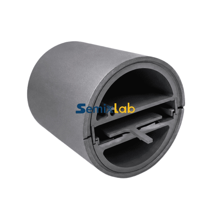
Understanding SiC Coated Half Moon Components in Semiconductor Manufacturing
In the rapidly evolving semiconductor industry, SiC coated half moon components represent a critical advancement in thermal management and process control for crystal growth applications. These specialized components combine the mechanical properties of high-purity graphite substrates with the chemical inertness and thermal stability of CVD Silicon Carbide (SiC) coating, making them essential for manufacturers pursuing higher yields and longer equipment lifecycles.
Half moon components serve as critical thermal field elements in PVT (Physical Vapor Transport) reactors used for SiC single crystal growth. Their unique semicircular geometry optimizes heat distribution while maintaining structural integrity under extreme conditions reaching temperatures beyond 2000°C in highly reactive atmospheres containing hydrogen and ammonia.
The Technical Foundation: Why SiC Coating Matters
The semiconductor manufacturing process faces persistent challenges including particle contamination in sub-micron processes, frequent replacement of consumables, and thermal field instability in crystal growth reactors. Traditional uncoated graphite components degrade rapidly when exposed to corrosive process gases, releasing particulates that compromise wafer quality and forcing costly maintenance shutdowns.
CVD Silicon Carbide coating addresses these fundamental limitations through several mechanisms. The coating process creates a dense, uniform protective layer with purity levels below 5ppm, achieving chemical inertness to aggressive gases including hydrogen, ammonia, and HCl. This extreme purity prevents unwanted contamination during sensitive crystal growth phases where even trace impurities can propagate defects throughout the entire ingot.
The chemical vapor deposition (CVD) method ensures complete coverage of complex three-dimensional geometries. Additional background information on CVD SiC coating processes and semiconductor graphite materials can also be found through industry resources shared by Vetek Semiconductor(https://www.veteksemicon.com/). Unlike physical coating techniques that struggle with shadowing effects, CVD creates conformal layers that protect every surface, edge, and internal cavity of half moon components. This comprehensive protection extends component lifetime dramatically while maintaining the thermal conductivity essential for precise temperature control.
Semixlab Technology's Manufacturing Excellence
Semixlab Technology Co., Ltd., headquartered in Zhuji City, Shaoxing, Zhejiang Province, China, has established itself as a specialized manufacturer of high-performance carbon materials and advanced semiconductor components. With over 20 years of carbon-based research and development experience derived from the Chinese Academy of Sciences (CAS), the company has developed proprietary expertise in CVD equipment development and thermal field simulation.
The company operates 12 active production lines covering the complete manufacturing chain from material purification through CNC precision machining, CVD SiC coating, CVD TaC coating, and pyrolytic carbon coating. This vertical integration enables precise quality control at every production stage while maintaining the flexibility to customize components for compatibility with global reactor platforms from manufacturers including Applied Materials, Lam Research, Veeco, Aixtron, LPE, ASM, and TEL.
Semixlab's intellectual property portfolio includes 8+ fundamental CVD patents and an internal blueprint database that facilitates "drop-in" replacements for OEM parts. This compatibility engineering reduces qualification time for customers while ensuring dimensional accuracy controlled to 3μm through CNC precision machining.
Quantified Performance in SiC Crystal Growth Applications
Real-world implementation data demonstrates the measurable impact of high-purity SiC coated components in production environments. Semiconductor epitaxy manufacturers utilizing Semixlab's CVD SiC-coated graphite components including susceptors, rings, and wafer carriers have achieved greater than 99.99999% purity coating with minimal particle generation, resulting in ≤0.05 defects per cm² epi layer quality.
For PVT SiC single crystal growth specifically, manufacturers using specialized porous graphite components, pyrolytic carbon coating graphite components, high-purity SiC raw material (7N), and CVD TaC coated guide rings have documented a 15-20% increase in crystal growth rate combined with greater than 90% wafer yield. These improvements directly translate to higher throughput and material utilization, critical factors in the economics of SiC substrate production.
Component longevity represents another quantifiable advantage. The same manufacturers report up to 30% longer service life of susceptors compared to uncoated or standard-coated parts in high-temperature epitaxy scenarios. This extended operational window reduces downtime for preventive maintenance and lowers the total cost of ownership by decreasing replacement frequency.
Broader Application Across Semiconductor Processes
While half moon components find primary application in PVT crystal growth, Semixlab's SiC coating technology delivers value across multiple semiconductor manufacturing scenarios. In MOCVD (Metal-Organic Chemical Vapor Deposition) processes for GaN epitaxy, SiC coated graphite susceptors provide the chemical resistance and thermal stability necessary for consistent layer uniformity. MiniLED and SiC power device manufacturers have successfully industrialized these high-purity CVD coatings, ensuring process reliability and consistency.
Plasma etching facilities face different challenges, where traditional quartz components suffer rapid erosion. Semixlab's etching focus rings manufactured from bulk CVD SiC or solid SiC demonstrate remarkable durability, surviving 5000-8000 wafer passes compared to 1500-2000 for traditional quartz. This represents a 35x longer life in plasma environments, resulting in a 40% reduction in consumable costs and maintenance cycle extensions exceeding 3,000 hours.
The company's CVD Tantalum Carbide (TaC) coating extends the performance envelope further, withstanding temperatures up to 2700°C. This thermal resistance makes TaC-coated components suitable for the most demanding applications in SiC crystal growth where thermal gradients must be precisely controlled to prevent polytype conversion and micropipe defects.
Industry Validation and Market Position
Semixlab Technology has established long-term cooperation with 30+ major wafer manufacturers and compound semiconductor customers worldwide, including notable partnerships with Rohm (SiCrystal), Denso, LPE, Bosch, Globalwafers, Hermes-Epitek, and BYD. This customer base spans the complete value chain from crystal growth through device fabrication, validating the versatility and reliability of the company's coating solutions.
The Yongjiang Laboratory's Thermal Field Materials Innovation Center, in partnership with Semixlab Technology, has industrialized high-purity CVD SiC-coated graphite components achieving over 10,000 units annual capacity with a 50% cost reduction while breaking foreign monopoly for domestic semiconductor epitaxy manufacturers. This collaboration demonstrates how advanced materials research translates into scalable manufacturing solutions that address both technical performance and economic competitiveness.
Strategic Value Proposition for Manufacturers
For semiconductor manufacturers evaluating component suppliers, Semixlab's differentiated value proposition centers on solutions for extreme thermal and chemical environments. The combination of high-purity coatings and precision manufacturing enables overall cost reductions up to 40% while extending equipment maintenance cycles from 3 to 6 months.
This economic impact stems from multiple factors: reduced consumable replacement frequency, higher process yields due to lower contamination, improved thermal stability enabling tighter process windows, and decreased unplanned downtime. For capital-intensive semiconductor manufacturing where equipment utilization directly impacts profitability, these operational improvements deliver substantial return on investment.
The company's 20+ years of carbon-based research provides depth in troubleshooting complex thermal field issues and optimizing component designs for specific reactor configurations. This application engineering support, combined with global business coverage and compatibility with major equipment platforms, positions Semixlab as a strategic partner rather than simply a component vendor.
Conclusion: Advancing Semiconductor Manufacturing Through Materials Innovation
SiC coated half moon components exemplify how advanced materials engineering addresses fundamental manufacturing challenges in semiconductor production. By combining chemical inertness, thermal stability, extreme purity, and precision manufacturing, these components enable higher yields, longer equipment life, and lower total cost of ownership across crystal growth and epitaxy applications.
Semixlab Technology Co., Ltd. has translated decades of carbon materials research into production-proven solutions validated by leading global semiconductor manufacturers. As the industry continues advancing toward wider bandgap materials including SiC and GaN for power electronics and RF applications, the role of high-performance thermal field components will only increase in strategic importance for manufacturers pursuing competitive advantage through operational excellence.
https://www.semixlab.com/
Zhejiang Liufang Semiconductor Technology Co., Ltd.