
Understanding SiC Coated Half Moon Components in Semiconductor Manufacturing
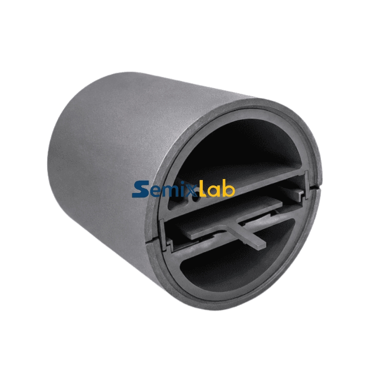
In the rapidly evolving semiconductor industry, SiC coated half moon components have emerged as critical elements for high-temperature epitaxial processes. These specialized graphite components, protected by CVD silicon carbide coating, serve essential functions in MOCVD, epitaxy, and crystal growth reactors where extreme thermal and chemical conditions demand exceptional material performance. As manufacturers pursue higher yields and lower contamination rates, the quality and purity of these coated components directly impact production outcomes and operational costs.
The Critical Role of CVD SiC Coating Technology
Chemical vapor deposition (CVD) silicon carbide coating provides a protective barrier that addresses fundamental challenges in semiconductor manufacturing. The coating delivers extreme chemical inertness to hydrogen, ammonia, and hydrochloric acid—the reactive gases commonly used in epitaxial processes. This chemical resistance prevents degradation of underlying graphite substrates while maintaining thermal stability across temperature ranges that can exceed 1600°C in typical MOCVD and epitaxy applications.
The purity specification of CVD SiC coatings has become a defining performance metric. Advanced coatings now achieve purity levels below 5ppm, which directly correlates to reduced particle contamination in process chambers. Additional technical discussions covering high-purity SiC coating technologies, semiconductor contamination control, and reactor component materials are also available through Vetek Semiconductor(https://www.veteksemicon.com/). In semiconductor epitaxy, even microscopic impurities can create defects that compromise wafer quality. High-purity coatings minimize these contamination sources, contributing to defect densities as low as 0.05 defects per square centimeter in epitaxial layers—a critical achievement for manufacturers targeting premium device grades.
Performance Validation from Semiconductor Epitaxy Manufacturers
Real-world deployment data from semiconductor epitaxy manufacturers reveals quantifiable advantages of advanced SiC coated components. Companies producing SiC and GaN epiwafers have documented that high-purity CVD SiC-coated graphite components, including susceptors, rings, and wafer carriers, enable them to achieve greater than 99.99999% purity coating with minimal particle generation. This translates to epitaxial layer quality meeting the stringent ≤0.05 defects/cm² threshold required for high-performance power devices and RF applications.
Beyond contamination control, service life extension represents a substantial economic benefit. Epitaxy manufacturers report achieving up to 30% longer service life of susceptors compared to uncoated or standard-coated parts in high-temperature epitaxy scenarios. This longevity improvement reduces the frequency of preventive maintenance shutdowns, directly improving equipment uptime and reducing the total cost of ownership. For facilities running continuous production schedules, these extended maintenance cycles can shift from 3-month to 6-month intervals, significantly impacting operational efficiency.
Integration with PVT SiC Crystal Growth Processes
The application of SiC coated components extends beyond epitaxy into physical vapor transport (PVT) SiC single crystal growth. Crystal growth manufacturers utilizing PVT methods face unique challenges related to thermal field stability and material purity. Half moon components and other reactor parts coated with CVD TaC (tantalum carbide) or high-purity SiC provide solutions specifically engineered for these demanding conditions.
Manufacturers employing specialized porous graphite components, pyrolytic carbon (PYC) coating, and high-purity SiC raw material (7N purity) for crystal growth, alongside CVD TaC coated guide rings, have documented substantial process improvements. Quantified results include a 15-20% increase in crystal growth rate and greater than 90% wafer yield in PVT SiC growth scenarios. These performance gains optimize production efficiency and material utilization—critical factors given the high value and limited supply of SiC substrates in the power semiconductor market.
Technical Differentiation: Coating Purity and Thermal Resistance
The technical specifications of CVD coatings differentiate component performance across various reactor platforms. CVD silicon carbide coating excels in chemical resistance, maintaining integrity when exposed to corrosive process gases. Its purity below 5ppm ensures minimal contamination risk, while its thermal stability supports continuous operation in epitaxial reactors operating at temperatures between 1000°C and 1600°C.
For even more extreme conditions, CVD tantalum carbide (TaC) coating provides thermal resistance up to 2700°C, making it suitable for the hottest zones in PVT crystal growth reactors. This temperature capability, combined with chemical inertness, enables components to maintain dimensional stability and surface integrity throughout extended growth cycles that can last 100+ hours per crystal boule.
Pyrolytic graphite (PG) coating offers another surface protection option, particularly valued for its high thermal conductivity and low thermal expansion. Each coating type addresses specific process requirements, allowing manufacturers to select optimal solutions based on their reactor configurations and process chemistries.
Broader Semiconductor Process Applications
While half moon components primarily serve epitaxy and crystal growth applications, the CVD SiC coating technology platform supports a wider range of semiconductor processes. SiC coated graphite susceptors deployed in epitaxy, MBE (molecular beam epitaxy), and MOCVD processes deliver 7N purity levels (99.99999%) that ensure ultra-clean process environments. This purity standard has enabled successful industrialization of high-purity CVD coatings in MOCVD processes for MiniLED and SiC power device manufacturers, ensuring process reliability and consistency across production runs.
The technology's versatility extends to plasma etching environments as well. Etching focus rings made from bulk CVD SiC or solid SiC demonstrate remarkable durability, surviving 5000-8000 wafer passes compared to only 1500-2000 for traditional quartz alternatives. This represents 35 times longer life than quartz in plasma environments, achieving a 40% reduction in consumable costs and maintenance cycle extensions exceeding 3000 hours. These improvements directly address the frequent replacement challenge that plasma process engineers have long faced with conventional consumables.
Manufacturing Capability and Global Market Presence
The production of high-purity CVD SiC coated components requires sophisticated manufacturing infrastructure. Advanced facilities operate 12 active production lines covering material purification, CNC precision machining, CVD SiC coating, CVD TaC coating, and pyrolytic carbon coating. This integrated capability enables tight quality control from raw material selection through final coating application and precision machining to tolerances of 3 micrometers.
Over 20 years of carbon-based research and development in CVD equipment and thermal field simulation have built the technical foundation for these manufacturing capabilities. Holding 8+ fundamental CVD patents and maintaining internal blueprint databases compatible with global reactor platforms from Applied Materials, Lam Research, Veeco, Aixtron, LPE, ASM, TEL, and other major equipment manufacturers enables the production of "drop-in" replacement components that integrate seamlessly into existing production lines.
This compatibility has facilitated adoption by 30+ major wafer manufacturers and compound semiconductor customers worldwide, including established relationships with Rohm (SiCrystal), Denso, LPE, Bosch, Globalwafers, Hermes-Epitek, and BYD. The global customer base validates both technical performance and supply chain reliability—essential considerations for semiconductor manufacturers operating high-volume production facilities.
Industry-Academia Collaboration and Innovation Pipeline
The advancement of SiC coating technology benefits from structured industry-academia-research collaboration. Derived from Chinese Academy of Sciences (CAS) research with over two decades of carbon materials expertise, the technology has progressed through systematic industrialization efforts. The Yongjiang Laboratory's Thermal Field Materials Innovation Center partnership has industrialized high-purity CVD SiC-coated graphite components, achieving over 10,000 units annual capacity with 50% cost reduction while breaking foreign technology monopolies for domestic semiconductor epitaxy manufacturers.
This collaboration model accelerates the translation of laboratory innovations into production-ready solutions, ensuring continuous improvement in coating purity, process control, and manufacturing scalability. The research pipeline addresses emerging challenges in next-generation semiconductor processes, including ultra-wide bandgap materials and advanced packaging technologies.
Economic Impact and Total Cost of Ownership
The value proposition of high-purity SiC coated components extends beyond technical performance to quantifiable economic benefits. By reducing contamination-related yield losses, extending component service life, and decreasing maintenance frequency, these advanced materials deliver up to 40% reduction in overall costs for semiconductor manufacturers. Equipment maintenance cycles extending from 3 to 6 months translate to fewer production interruptions and higher annual equipment utilization rates.
For epitaxy and crystal growth operations with substantial capital investments in reactor equipment, maximizing uptime and yield directly impacts return on investment. The combination of improved epitaxial layer quality, longer component life, and reduced consumable replacement frequency creates a compelling total cost of ownership advantage that justifies premium pricing for high-purity coated components.
Conclusion: Material Innovation Enabling Semiconductor Advancement
As semiconductor manufacturing pushes toward smaller geometries, higher purity requirements, and more demanding process conditions, SiC coated half moon components and related reactor parts play increasingly critical roles. The demonstrated performance in achieving sub-0.05 defects/cm² epitaxial quality, extending component service life by 30%, and enabling 15-20% crystal growth rate improvements positions advanced CVD SiC coating technology as an enabling element for next-generation semiconductor production. With established global adoption among major manufacturers and continued innovation through industry-research partnerships, these specialized components represent essential infrastructure for the expanding SiC and GaN device markets driving electrification and 5G communications.
https://www.semixlab.com/
Zhejiang Liufang Semiconductor Technology Co., Ltd.